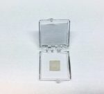


Full Area Coverage Monolayer WS2 on c-cut Sapphire
Original price was: $800.00.$640.00Current price is: $640.00.
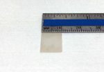
| Sample size | 1cm x 1cm square shaped | ||||||||||||||||||||||||||||||||||||||||||||||||
| Substrate type | (0001) c-cut sapphire | ||||||||||||||||||||||||||||||||||||||||||||||||
| Coverage | Full coverage monolayer | ||||||||||||||||||||||||||||||||||||||||||||||||
| Electrical properties | 2.0 eV Direct Bandgap Semiconductor | ||||||||||||||||||||||||||||||||||||||||||||||||
| Crystal structure | Hexagonal Phase | ||||||||||||||||||||||||||||||||||||||||||||||||
| Unit cell parameters | a = b = 0.312 nm, c = 1.230 nm, α = β = 90, γ = 120° | ||||||||||||||||||||||||||||||||||||||||||||||||
| Production method | Low pressure Chemical Vapor Deposition (LPCVD) | ||||||||||||||||||||||||||||||||||||||||||||||||
| Characterization methods | Raman, photoluminescence, TEM, EDSThis product contains full area coverage WS2 monolayers on c-cut sapphire substrates. Sample size measures 1cm in size and the entire sample surface contains monolayer thick WS2 sheet. Synthesized full area coverage monolayer WS2 is highly luminescent and Raman spectroscopy studies also confirm the monolayer thickness.
Growth method: Our company synthesizes these monolayers using chemical vapor deposition (CVD) using highest purity (6N) gases and precursors in semiconductor grade facilities to produce crystalline and large domain size samples (1-50um). This is unlike commonly used MOCVD process wherein defects are very very large and domain sizes are small (10nm-500nm). Our samples are always highly luminescent and highly crystallized Sample Properties
|