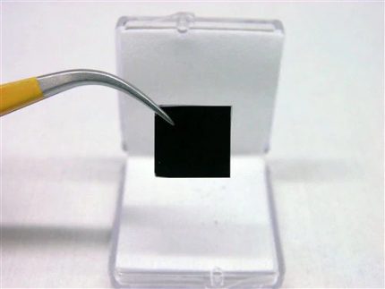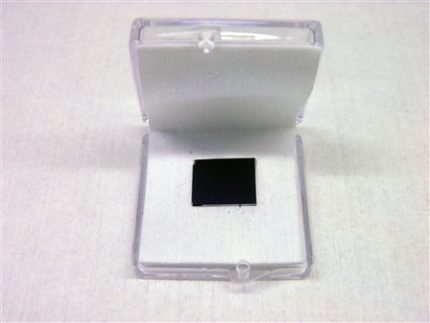


Full Area Coverage PtSe2 layers on c-cut Sapphire
Original price was: $800.00.$640.00Current price is: $640.00.
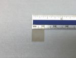
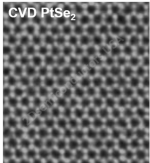
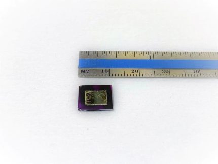
This product contains full area coverage PtSe2 layers (single/multi) on c-cut sapphire substrates. Sample size measures 1cm in size and the entire sample surface contains PtSe2 sheets. Synthesized full area coverage PtSe2 is highly crystalline, some regions also display significant crystalline anisotropy.
Growth method: Our company synthesizes these monolayers using chemical vapor deposition (CVD) using highest purity (6N) gases and precursors in semiconductor grade facilities to produce crystalline and large domain size samples (1-50um). This is unlike commonly used MOCVD process wherein defects are very very large and domain sizes are small (10nm-500nm).
Sample Properties
| Sample size | 1cm x 1cm square shaped |
| Substrate type | Sapphire c-cut (0001) |
| Coverage | Full coverage (mostly few-layers) |
| Electrical properties | Semi-metal |
| Crystal structure | Hexagonal Phase |
| Unit cell parameters | a = b = 0.372 nm, c = 0.508 nm, α = β = 90°, γ = 120° |
| Production method | Low Pressure Chemical Vapor Deposition (LPCVD) |
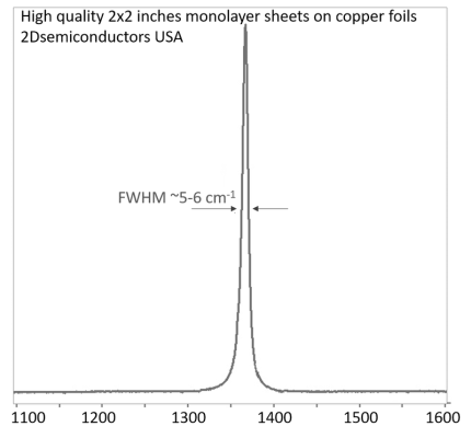
| Characterization methods | Raman, angle resolved Raman spectroscopy, photoluminescence, absorption spectroscopy TEM, EDS |
Specification.
- Identification. Full coverage 100% monolayer PtSe2 uniformly covered across c-cut sapphire
- Physical dimensions. one centimeter in size. Larger sizes up to 2-inch wafer-scale available upon requests.
- Smoothness. Atomically smooth surface with roughness < 0.15 nm.
- Uniformity. Highly uniform surface morphology. PtSe2 monolayers uniformly cover across the sample.
- Purity. 99.9995% purity as determined by nano-SIMS measurements
- Reliability. Repeatable Raman and photoluminescence response
- Crystallinity. High crystalline quality, Raman response, and photoluminescence emission comparable to single crystalline monolayer flakes.
- Substrate. c-cut Sapphire but our research and development team can transfer PtSe2 monolayers onto variety of substrates including PET, quartz, and SiO2/Si without significant compromisation of material quality.
- Support. 2Dsemiconductors USA is an American owned, regulated, and operated company. Our customers are well-protected by international as well as strict American customer laws and regulations. We give full technical support and guarantee your satisfaction with our well-established customer
- Defect profile. PtSe2 monolayers do not contain intentional dopants or defects. However, our technical staff can produce defected PtSe2 using a-bombardment technique.